Relay Board Conversion
A project that converts a parallel-port relay board to a serial shift-out
interface.
The AVIOSYS AK28 relay board is a kit originally designed for a PC
parallel port interface. Parallel ports are becoming quite rare, and
newer PC operating systems make it quite hard to get direct access the the
hardware for manipulating the ports for custom hardware. Also, MCUs
like the Arduino don't easily support a parallel port interface. In
order to make the board usable with a MCU it was upgraded from parallel
port to serial shift-out.
A serial shift-out interface uses the 74HC595 (or similar) serial-to-parallel shift
register, which is very widely used for Arduino-compatible devices. This
device takes a serial stream of 8 bits of data, stores them in a register
and makes the data available to an external device with one bit per output
pin. A useful feature of the '595 is that the output pins do not
change until the data input is completed, so intermediate values that
occur as the data is being streamed in do not appear at the output
pins. A common use is for a 7-segment LED display where the value is
loaded from the serial input and converted to parallel form for driving
the display. Obviously, this functionality is suitable for replacing
a parallel-port interface. The chip uses just three signals with the
Arduino - a data signal that sets the bit values (in sequence), a clock
signal that indicates when the bit value has been set and pushes it into
the shift register, and a latch signal that marks the ends of the data
stream. The timing for the various signals is very flexible so it is
easy to program. The chip has other features that are not used in
this example. Note that the 'HC' version of the chip is probably the only
one currently available, but the chip is frequently recovered from old
equipment, and other versions such as "S", "LS" or "F" will work
just as well.
Modification
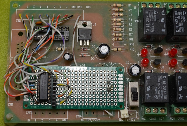
 The
AVIOSYS AK28 is a relay board with eight 9V relays which are driven from a
8-12V input. Each relay has its own driver and indicating LED. There
was an option for powering from a mains supply which was never installed
for this example. The original interface featured a 25-pin 'DB'
connector for connection to the parallel port of the PC. Custom software
was supplied for sending data to the PC printer port and setting the port
control pins as required for the board interface. The upgrade
involved removing the connector and the interface chip, and wiring a small
daughter board with the 74HC595 through to some convenient pads that
correspond to the 8 data pins of the parallel port, plus pin 14 from the
original interface chip for power. The daughter board was supported
with some single-strand copper wire staked to several convenient
thru-holes on the board. The original supply for the logic was from
the regulated 6V provided for the relay drivers, via a diode, giving just
over 5V at the chip.
Schematic

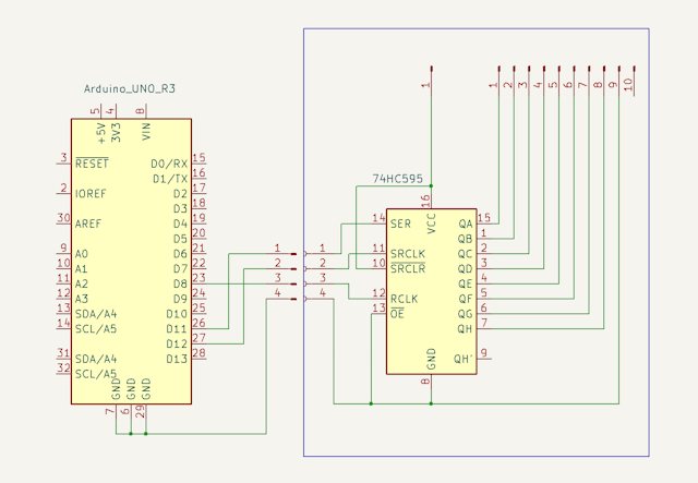
The daughter board consists of the 74HC595 and a 4-pin header for the
connection to the Arduino. The data outputs from the 74HC595 are
connected to the 8 thruholes corresponding to the data pins of the
parallel connector. The VCC pin of the 74HC595 is wired to a convenient
thruhole that has 5V from the on-board regulator. In this example
the 74HC595 is socketed, and the header is actually 7 pins, to allow for
connection to the unused 74HC595 pins plus an extra ground if that should
be required for some reason.
The Arduino pins listed here correspond to the pins used for the examples
referenced below. No special handling is associated with these pins,
and any GPIO pin that can be configured as an output could be used.
The terminology varies somewhat, but SER is the data, RCLK is the clock
for the shift register, and SRCLK is the latch, or the 'clock' for the
storage register.
The data loading sequence is:
Set the latch to LOW so that the storage contents will not change as the
data is streamed in.
Set the data to the first required bit value.
Pulse the clock.
Repeat setting the data and pulsing the clock for the remaining 7 bits
Set the latch to HIGH to transfer the shift register to the storage
(output) register.
In the examples referenced below the process of setting the value of each
bit and pulsing the clock is handled by an inbuilt routine, using a 8-bit
value prepared beforehand, also using an inbuilt routine.
Sample Code
Note that the 74HC595 is a 'device
that’s clocked by rising edges'.
Note that the tutorial example 1.2 is
the best one to use for the AK28. Be sure to set the console
to "No Line Ending" so that the character handled by the routine is the
character that was typed, not the line ending character!
The examples use the the three-wire interface, so the outputs do not
change until the rising edge of the latch signal, after the shift register
has been loaded. There are many examples available where the latch
is held high. With this simplified arrangement the outputs will
change as the data stream is serialized into the register. For a
bank of relays the latch signal should always be used - if the outputs are
allowed the change rapidly the relays may chatter, and current consumption
will increase.
This site was last updated 7th August 2024.

 The
AVIOSYS AK28 is a relay board with eight 9V relays which are driven from a
8-12V input. Each relay has its own driver and indicating LED. There
was an option for powering from a mains supply which was never installed
for this example. The original interface featured a 25-pin 'DB'
connector for connection to the parallel port of the PC. Custom software
was supplied for sending data to the PC printer port and setting the port
control pins as required for the board interface. The upgrade
involved removing the connector and the interface chip, and wiring a small
daughter board with the 74HC595 through to some convenient pads that
correspond to the 8 data pins of the parallel port, plus pin 14 from the
original interface chip for power. The daughter board was supported
with some single-strand copper wire staked to several convenient
thru-holes on the board. The original supply for the logic was from
the regulated 6V provided for the relay drivers, via a diode, giving just
over 5V at the chip.
