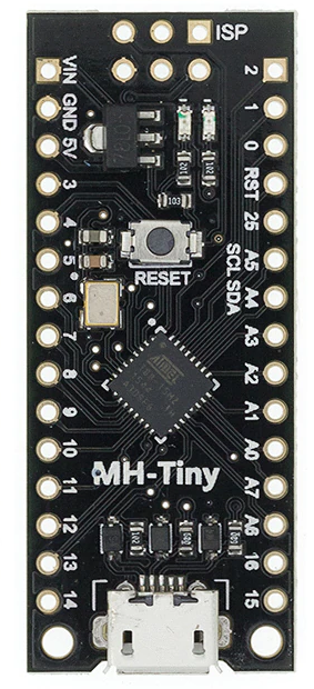
The ATTiny88 is somewhat of an oddball in the MCU environment. It is in the Atmel AVR family, but it has very limited memory (8K bytes flash, 64 bytes EEPROM and 512 bytes SRAM) and only 2 timers. But it has a huge number of GPIO pins - up to 28 depending on the package. It supports I2C, ISP and PWM (2 pins), but has no hardware UART.
It is available as a very small and inexpensive module, with very few additional features. In fact, just about the only things on the module apart from the MCU are a 5V regulator, a pair of LEDs, a reset button and the USB socket.
The purpose of this project is to see what is involved in using the ATTiny88 module as a dedicated I2C interface so that a reasonably complex standalone piece of hardware can be controlled through I2C.
The stand-alone device chosen for the project is a keypad/display module. It contains 16 push buttons, organised as a 4x4 matrix, 4 individual push buttons, and 8 LEDS.
The 4x4 matrix requires 8 GPIO lines to drive it, while the 4 buttons and
8 LEDS require one each, for a total of 20 pins. I2C takes up two
more, and during development 2 pins are required for a software UART for
monitoring and debugging. With 28 pins available, that arrangement
is possible, but there's not much room for further growth. For this
project, the LEDS are driven with a 74LS164 shift register, so only three
pins are required, reducing the total used for the hardware. The
74LS164 also has the advantage of buffering the LED drive, ensuring that
the current draw on the ATTiny88 is kept within specs even with all LEDS
fully on.

ATTiny88 Module is available from multiple sources. The form factor is very similar to a Nano. There is a guide to using it with the Arduino IDE here. Note that there are several versions of the support driver software for Windows available and not all of them work with 64-bit Windows 10 or later. Chinese versions of the module appear to be identical, except that "MH-" has been deleted from the board.
Analog pins A0 to A7 are accessible as digital input and output using numbering that runs from 17 to 24 as implied by the board labels. (Using the 'Ax' form of reference in code is not recommended as not all versions of the MCU package implement the pin number calculation correctly.) The LED is on pin 0. SCL and SDA are marked for the I2C interface (A4 and A5). The serial monitor is installed using D3, D4 by default, but as it is a software serial port, any pair of pins would be suitable. Hardware PWM is on pins 9 and 10 which have been avoided in this example. (The chip only has two timers and these pins are the only ones that support hardware PWM.)
The module supports a USB interface for programming, but there is no separate USB controller. The MCU contains a bootloader that interacts directly with the USB driver on the desktop to download and install the program. At each boot the bootloader looks for the driver. If the driver is not detected, or if it is detected but there is no program download pending, the bootloader starts the user code. If a program download is pending the bootloader puts the MCU into download mode and the program is downloaded. When downloading a program is complete the user code is started. This implies that to download software the ATTiny should not be connected to the PC until after the download has been initiated. However, although the prompt from the downloader to indicate that a download is pending instructs the user to connect the MCU to the USB port, it is actually sufficient just to reset the MCU.
This programming arrangement means that the USB port is not available as a serial port during program development - it is claimed by the driver on the PC. The simplest option to provide debugging support is to create a software serial object in code and connect a suitable serial device at pins 3 and 4. If a UART-toUSB device such as an ESP01 programmer is used then the port can be selected in the Arduino IDE so that the IDE console can be used for debugging, as if the MCU were connected to that port. Only one copy of the IDE is needed - the USB port used for the software serial monitor can be nominated as the connection port because that setting is ignored by the driver during program upload. The result is a configuration that looks the same as other devices such as UNO, except for the need to press reset to start the download. A PC terminal program such as PUTTY driven from the PC serial port or through a serial to USB adapter would also work. A device that can provide input as well as display debugging information might be required, depending on the application - in this example it was essential for the Master device to be available in order display the key-presses and select a LED.
The usable memory of the ATTiny88 is severely restricted because of the space taken up by the bootloader. This project uses about half the available program memory. However, if a software serial object is created then the program memory usage rises to about 80%, so there is limited room for expansion if a monitor required for debugging uses a serial interface. ISP is supported, and might provide an alternative debug interface with less memory usage, but it was not tested for this project. I2C could also be used, with a I2C to UART converter (with a different ID).
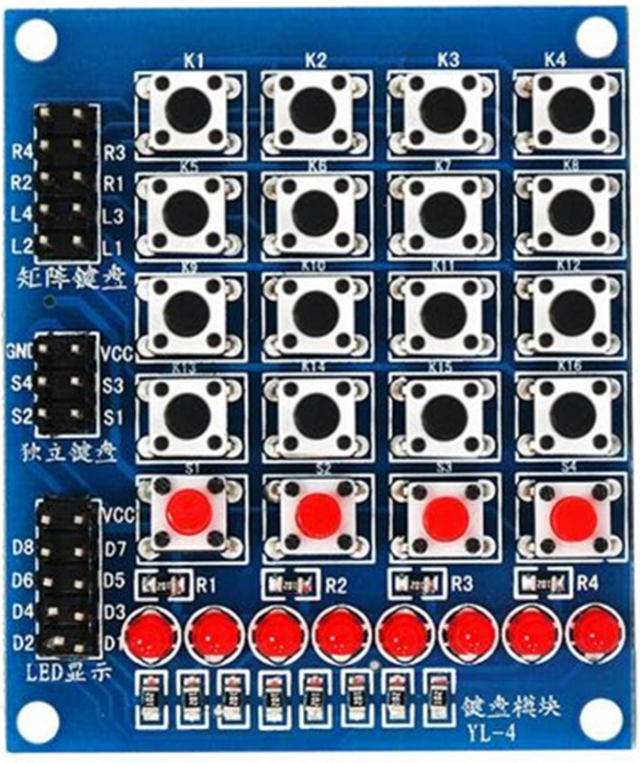 4x4 matrix keypad
with 4 extra buttons and 8 LEDS.
The connection to the keypad used in this example is:
74164 shift register:
Function Module 74164
Clear Pin
11 ~CLR(9)
Clock Pin
12 CLK(8)
Data Pin
13 A, B(1, 2)
D1-D8
QA-QH(3,4,5,6,10,11,12,13)
(74164 pin numbers are for the 14-pin DIP. Other packages will differ.)
4x4 Key Matrix and 1x4 buttons:
Function Module
R1 17 (A6)
R2 20 (A1)
R3 18 (A7)
R4 19 (A0)
L1 16
L2 22 (A3)
L3 15
L4 21 (A2)
S1 6
S2 5
S3 8
S4 7
(Pin usage for the keys and buttons was partly determined by the layout of the ribbon cable, and is easily adjusted in the code if different pins are used.)
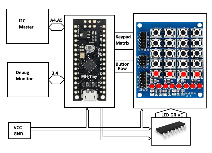
A master I2C device is required for testing the slave. The master will issue commands to turn the LEDs on and off, and will display the key and button codes as they are pressed, so it must have an attached console. The master can be any MCU that supports I2C. Code for the master is included below and should work correctly for any MCU that supports I2C. For this example it was a UNO, but the code has also been tested in a Nano and should work for any MCU supported by the Arduino IDE. It won't fit in a ATTiny88 (mainly due to the space required for software serial).
All commands require three characters, formatted as command (0 to 9 decimal) and value (0x00 to 0xFF, 2-character HEX). The invert command does not use the value, but it is required for input parsing. Input line termination can be CR, NL or both. There is no input validation other than a minimum three characters. Invalid commands might produce strange results.The master uses the I2C transmission to send LED commands to the slave. The request is simply passed through from the user, with the HEX input converted to a byte: that is, 2 bytes consisting of command and value.
The master uses I2C Request to request the keypress information from the slave. Requests are sent in the main loop with a small delay, which effectively handles any key bounce that might have occurred in the slave. If no key has been pressed since the last request 0xFF is returned from the slave.
The slave uses the I2C Receive event to listen for LED commands. The command and value are stored and a flag is set. The next time the loop executes it sees the flag set and executes the command by updating the LED's status byte and writing it into the shift register.
The slave uses the I2C On Request event to respond to a request for a key code. If a key has been pressed since the last request was received then the code for the key is returned as two bytes - row and column (0-3/03 for the 4x4 matrix, 4/0-3for the switches). If no key press has occurred the slave returns 0xFF.
The key and button scanning has been kept simple. If a key and a button have both been pressed the button will be returned. If two keys or two buttons are pressed the first one in row/column scan order will be returned. Any subsequent button press before the next request from the master is received overwrites the previous press. An interesting improvement would be to queue the presses up and release them one by one as the requests are received. For this example it is unlikely that a user could press buttons faster then they are processed, but for other devices it is possible that data could be missed if it's not queued.
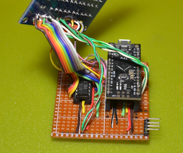 The keypad/LED board is modified by removing the headers. This is
necessary because the button height should be kept to a minimum in order
to maintain stability of the finished unit. The simplest way to
remove them is to lever off the plastic base of the headers (a small
amount of heat may be necessary) and then unsolder the pins one at a time.
Clean the thru-holes with solder wick.
The MCU and the shift register are mounted to a piece of stripboard cut to match the size of the matrix board. Sockets are optional but have been used in this example so that some of the wiring can be run under the socket, making connection of the matrix wiring a little simpler. The MCU is positioned so that the USB port is at an edge, and 5V, GND, SDA and SCL are brought out to a 4-pin header at the side.
This arrangement means that power can be provided either as part of a 4-wire I2C connection to the master device or separately through the USB port. Both sources should not be used simultaneously. However, if power is provided through the USB port it may still be necessary to include a GND to the master as part of the I2C connection.
Wiring should be kept light and flexible so that the parts can be easily handled while soldering and during installation in a case.
In this example the positioning of the components has not considered an allowance for supports for the matrix board passing through the stripboard - support has been arranged with structures within the case. Stacked standoffs from the base, through the stripboard, might be a simpler way to arrange the mounting.
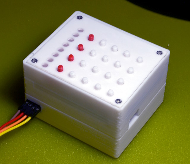
The case is made up of three layers - a base, a riser section and a lid. The lid sits on standoffs on pads set into the riser section, while the stripboard sits on its own pads in the base section. In order to get all the buttons and standoffs aligned the board and standoffs were held in place with some hot glue while the buttons were placed into the lid from the rear, and the body carefully lowered onto the lid before screwing it into place.
The buttons have a square base with a dimple to keep then centred on the swtich. As the dimple does not print well due to support material, each one was gently reamed out to a smooth finish using a 'corn' milling cutter.
The address of the slave unit is defined in the code as 0x08, but any available address could be used. Addresses in the range 00-07 are usually avoided. The I2C bus specifies that pull-up resistors should be used on the SDA and SCL lines. The calculation of the value of these resistors actually depends on the devices using the bus and the capacitance of the interconnections - I2C is not generally used as a pluggable bus and there is no mechanism for varying the pullups for the particular devices that happen to be connected. The pullups are also typically located close to the master device, but as this project is designed for temporary use with a variety of master devices, that would be impractical. The best compromise is probably a resistor of 3.3KΩ ~ 10KΩ close to the connecting header, and keeping the connecting cables short.
Each command is two bytes - command and value. For some commands value is not used. A terminator (CR and/or LF) is required. The I2C address is hard-wired in the code and is not required as part of user input.
0 Clear Single. Value is a LED number (0 to 7). The LED
is turned off.
1 Set Single Value is a LED
number (0 to 7). The LED is turned on.
2 Clear Value (OR) The value is a bit pattern (00 to FF). Each
LED corresponding to a '1' bit is turned off.
3 Set Value (OR) The value is a bit pattern
(00 to FF). Each LED corresponding to a '1' bit is turned on.
4 Set Value The value
is a bit pattern (00 to FF). Each LED is turned on if its bit is '1', or
turned off if it's '0'.
5 Invert
Each LED is turned on if currently off, and off if currently
on.
6 Rotate Left 1-bit position - value
is ignored.
7 Rotate Right 1-bit position - value
is ignored.
8 Shift Left
The LED pattern is shifted one place to the left. If value is
odd then the right-most LED is turned on.
9 Shift Right The LED
pattern is shifted one place to the right. If value is odd then
the left-most LED is turned on.
0,0 0,1 0,2 0,3
1,0 1,1 1,2 1,3
2,0 2,1 2,2 2,3
3,0 3,1 3,2 3,3
4,0 4,1 4,2 4,3
This page last updated 28th August 2024
