LED Array Test Box Project
This simple project is a little test box that includes 6 LEDs that can
be safely driven from the GPIO ports of any MCU. The device is
very useful for quick testing of prototypes - a few lines of code can
drive LEDs on any spare pin of the prototype to provide a visual
indication of what it is doing. I tend to set up these indicators
and leave them largely unchanged, and use the serial monitor for detailed
debugging information. It works like a very simple logic
analyzer.
The box has connections for 5v and Gnd, and an input pin for the six
LEDs. The inputs are buffered so that the load on each input is
about 1.6mA each: that is well within the 20mA per-pin maximum of the
Arduino UNO, and also well within 200mA total for all pins.
Parts
DM/SN7407 Hex buffer, or similar (eg, 7417)
6 x LEDs with dropping resistors to suit. This project uses bright
white LEDs with 150Ω resistors. Standard red or green LEDs typically use
220Ω or 330Ω resistors.
Prototype board approx. 4cm x 6cm. Many styles would work.
Headers: 2 x 3-pin, 1 x 6-pin.
3D printed case.
DM/SN7407 Integrated Circuit
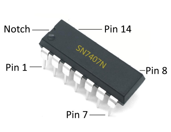 The 7407 medium-scale integrated circuit is a hex
buffer/driver with open collector outputs. Hex simply means there
are six separate buffers/drivers within the chip. Open collector
means that the output is a transistor switch - on or off - that switches
the supply from some external source to ground. In this case the
external voltage source is actually the same 5v supply that powers the
chip, but in other applications it could be a supply of up to about
30v. The maximum current for each switched circuit is 40mA - well
within the 20mA typically required for a LED. These chips are easily
recovered from obsolete equipment - they are large enough to solder with a
typical hobby soldering iron, but small enough to fit into a suitable
device case. Note that there are several variations of this chip, such as
'LS' and 'S', and also 5407 which is a lower voltage military version: any
of these variants is suitable for this project.
Note that the notch at the end of the chip defines the pin
numbering. With the notch at the left-hand end, looking from above,
pin numbers start at the lower left-hand corner and proceed
anti-clockwise. The lettering is usually aligned with the notch at
the left, but do not rely on it.
THE CIRCUIT
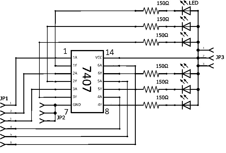 Pins 7 and 14
of the 7407 are connected to the ground and +5v 3-pin headers
respectively. The 6-pin input header JP1 is connected to the input
pins (1A through 6A) of the 7407, while the output pins (1Y through 6Y)
are connected via resistors to the LEDs and then to the LED driver voltage
at JP3. When the logic level at the input of the 7407 is high then
the corresponding transistor switch turns on and connects the LED to
ground through the GND (pin 7, JP2) of the 7407.
In this configuration the LED driver voltage is the same as the 7407
supply voltage, that is, 5V at pin 14. The alternative arrangement
is to disconnect JP3 from pin 14, supply 5V separately to pin 14, and
connect the alternate LED supply voltage to JP3. This alternate
supply must be no greater than 30V, and LEDS+resistors, or relays or
whatever other device is used must be capable of handling the higher
voltage. There must be a common ground between each supply, the test
unit and the MCU.
ASSEMBLY
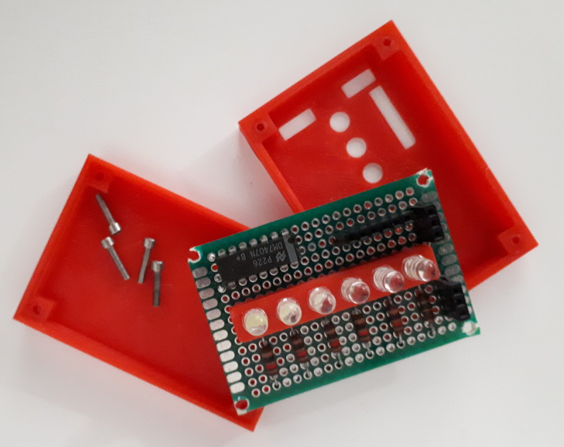
The parts are laid out on the prototyping board in a form that keeps the
wiring as simple as possible. In this example I have placed the LEDs
across the middle, with their resistors running to a buss at the
top. The +5v and Gnd headers are off to one side, and the input
header is aligned below the LEDs. The board can then be wired
point-to-point on the underside. The hookup wire came from an old
parallel printer cable. This wire is easily tinned and soldered, the
covering is very heat resistant, it is quite flexible, and the multitude
of colours means that the wire can indicate the function of the
connection, reducing the risk of mistakes. Note that I printed a standoff
for the row of LEDs - this helped to keep them properly aligned for height
and position.
The case is a simple two-part assembly, with a base
that the prototyping board sits down into, and which then screws through
countersunk holes from the back into standoffs in the lid. The lid
has cutouts for the LEDs and the headers. The screws self-thread into the
holes in the lid - a solution that is adequate for such a small case. The
screws were slightly too big for the holes in the prototyping board: the
corners could be cut away completely because the board is held securely
between the base and the lid.
COMPLETED
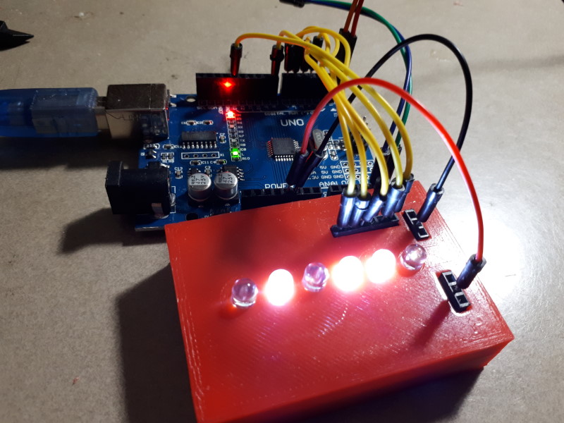
The completed unit, with the lid screwed onto the base and connected to a
UNO. There ar small markings molded into the lid to identify the +5v
and Gnd headers, but it doesn't show in the images. To use the
unit, +5v and Gnd connections are plugged in the respective headers, and
then output pins from the MCU are connected to the input header. When
the output is high the LED is lit. The +5v and Gnd headers
provide a convenient point for taking off connections to other items being
tested.
If the +5v supply does not come from the Arduino then it is critical that
the GND from the test unit is connected to the Gnd on the Arduino.
 This site was last updated 6th
August 2024.
 The 7407 medium-scale integrated circuit is a hex
buffer/driver with open collector outputs. Hex simply means there
are six separate buffers/drivers within the chip. Open collector
means that the output is a transistor switch - on or off - that switches
the supply from some external source to ground. In this case the
external voltage source is actually the same 5v supply that powers the
chip, but in other applications it could be a supply of up to about
30v. The maximum current for each switched circuit is 40mA - well
within the 20mA typically required for a LED. These chips are easily
recovered from obsolete equipment - they are large enough to solder with a
typical hobby soldering iron, but small enough to fit into a suitable
device case. Note that there are several variations of this chip, such as
'LS' and 'S', and also 5407 which is a lower voltage military version: any
of these variants is suitable for this project.
  Pins 7 and 14
of the 7407 are connected to the ground and +5v 3-pin headers
respectively. The 6-pin input header JP1 is connected to the input
pins (1A through 6A) of the 7407, while the output pins (1Y through 6Y)
are connected via resistors to the LEDs and then to the LED driver voltage
at JP3. When the logic level at the input of the 7407 is high then
the corresponding transistor switch turns on and connects the LED to
ground through the GND (pin 7, JP2) of the 7407.

 This site was last updated 6th
August 2024.