Parallel-in Serial-out Shift Register
An example of using the 74166 Parallel-in Serial-out shift
register to aggregate a multi-position switch for input to a MCU.
The project is an example of how to use the 74166 parallel-in, serial-out
shift register to convert multiple digital signal lines into a single
serial data stream. The example uses two 74x166 ICs to provide 16 inputs
on the single serial line. This requires just three GPIO pins at the
MCU to handle the 16 inputs. Expanding the inputs with additional 74x166
devices can be done with a simple change to the code and would not require
any more GPIO pins.
The example uses single-pole 6-position rotary switches as the source of
the digital inputs, together with an example SPST switch.
Parts:
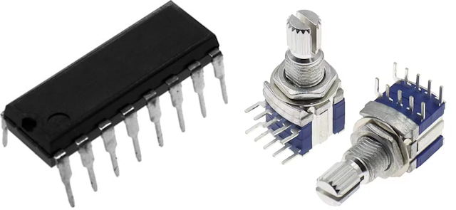 Arduino UNO. Any similar MCU
would work, as the code does not use any special features. A 3.3V
device will require a level shifter for the three connections to the
74x166, and the digital inputs will need to provide 5V logic levels to the
74x166. A very fast MCU might need additional delays to allow for
setup times.
74x166 Parallel to Serial Shift Register. This is available in
several different formats. There is an A version with sligtly different
electrical characteristics, but there should be no difference between the
versions in this application.
2x single pole 2-position switches, for providing test input
signals. Any other mechanism for providing different inputs to the
74x166 would be suitable. The schematic shows how a SPST switch
would be configured.
Prototyping board, hookup wire. The board should be sized to be
clear of the USB and power connectors at the end of the UNO, to provide
maximum options for positioning.
Schematic
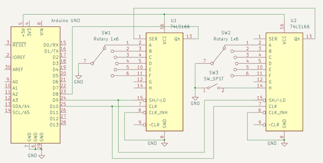 The
schematic shows the setup for an Arduino, but any MCU would be essentially
the same. The prototype was built with two 74x166 devices, two
single pol 6 position switches and one SPST switch to drive the inputs.
The clock and data inputs to the 74x166 devices are wired in parallel,
with the serial output of the second device fed back to the serial input
of the first. The serial output of the first is then fed back to the MCU.
Code
The code does not use any libraries. The pinout for the Arduino is
described in the code and the schematic, but any convenient GPIO pins
could be used, provided the code is adjusted. Timing is not
critical, but sequencing is. The TI data sheet for the device does
not include a lot of detail, the timing diagram appears to be incorrect,
and the description is confused by the failure to clearly distinguish
between operation with or without a free-running clock.
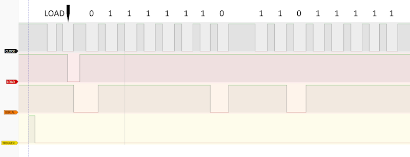
The TI documentation seems to be inconsistent with the actual behaviour
of the device. The clock low-to-high transition that occurs while
LOAD is low appears to be required in order to force the loading from the
parallel inputs. However this transition is also the first
transition for the data shifted out from the serial register. The
documentation indicates that this first transmission occurs after LOAD
goes high. The discrepancy can be ignored if the clock is maintained
low until the first bit of the serial data is tested. The result is that
the subsequent bits are tested with the clock low, and there is an
additional low-to-high transition at the end of the sequence.

Code
Download

 Arduino UNO. Any similar MCU
would work, as the code does not use any special features. A 3.3V
device will require a level shifter for the three connections to the
74x166, and the digital inputs will need to provide 5V logic levels to the
74x166. A very fast MCU might need additional delays to allow for
setup times.
  The
schematic shows the setup for an Arduino, but any MCU would be essentially
the same. The prototype was built with two 74x166 devices, two
single pol 6 position switches and one SPST switch to drive the inputs.